Background
For many radio applications, antenna operation at resonance across multiple frequency bands is highly desirable and has been the holy grail for many decades. The Switched Multi-Band Antenna (SMBA) is designed to operate over multiple bands at resonance and low SWR’s without having to make efficiency and other tradeoffs to achieve multi-band operation. These antennas can be used in amateur radio, commercial radio, and military applications.
The SMBA employs a wireless switching device that utilizes nonconductive, wireless control signals delivered to the physical antenna switching devices, latching relays, to create resonant operation. Fiber optics are used to deliver remote wake-up signals and control information to the switching devices that reconfigure the antenna system for resonant operation on each desired frequency band. For amateur radio, it is envisioned that SWBA techniques can be used to turn most common monoband antenna designs into corresponding multiband designs by inserting switching devices into the antenna elements.
An earlier design attempted to create a purely autonomous, self-regenerating, wireless switching device that could automatically sense RF signal presence, perform frequency counter operations to determine the RF transmit signal frequency present on the antenna, then make a switching decision to reconfigure the antenna elements. It also contained an energy harvesting circuitry design to recharge its battery, including harvesting RF from the antenna itself, combined with small solar panels, to recharge the system indefinitely. The microcontroller had a low-power sleep mode that consumed about 10 uA when sleeping and used up to 5 mA whenever RF was present.
A lot was learned from this early prototype. First, it definitely proved that switching devices could, in fact, be inserted effectively into the antenna elements and used to achieve resonant operation, without causing significant negative side effects on antenna operation. It also showed that operationally, having to key down to tune the antenna from RF sensing, at a lower tuning power level, for each band change, was problematic and very inconvenient. It took 4 seconds of RF to signal that a band switch was desired. The frequency counter worked fine. However, it turns out that 10 uA is still far too much quiescent current for reliable long-term operation. The voltage regulator and other components required also drew power (which wasn’t adequately accounted for), so the entire design failed to meet design objectives, due to excessive power requirements and a short battery duration of just a few weeks’ time (instead of years).
The other major issues involved the RF harvesting and RF sensing scheme. Because the design required incoming RF signal sampling directly from the antenna, and the MCU had to operate during RF transmit operation, the PCB ground was swimming in RF EMI, which would sometimes cause the MCU to reset. Various attempts to filter the RFI failed, as the MCU had to operate within the extremely strong electromagnetic fields of the antenna near-field, and required RF samples had to be loosely coupled into the frequency counter circuity. The RF harvesting sometimes worked, sometimes didn’t. The amount of RF required to run the frequency counter was high enough that it would sometimes cause the MCU lockup issues. In the end, these multiple issues resulted in the design failing to meet its original goals. But in failure there is learning. The key is not giving up, but learning, iterating, and pressing forward relentlessly.
Things that worked well included the latching relay’s switching of the antenna segments, the use of an MCU to make intelligent switching decisions, and the use of DIP switch settings to configure each switching device to operate autonomously to make its own proper switching decisions. Another lesson learned was the use of switched power, whereby the MCU switches power on/off for certain circuitry that normally draws too much quiesce power.
Other options that were evaluated included the use of low-power wake-up receivers (WuRx) to wake up an MCU from a low-power sleep state, to send the higher power MCU the switching information remotely. Unfortunately, the state of the art at this time for WuRx technology remains too limited – available techniques either take too much power due to active pre-amps to improve sensitivity and remote-control distances or operate at lower power levels (usually 10 or more microwatts) but then suffer from distance limitations of just a few meters.
At every step of the way, the biggest challenge was always rooted in keeping power consumption low during lengthy idle periods, the state in which antennas spend most of their lives (not in use).
The Switched Multi-Band Antenna
The Switched Multi-Band Antenna implements a multi-band antenna capable of operating across two or more frequencies at resonance using switching devices that are remotely controlled via plastic fiber optic signals. It turns out that fiber optics were the key to achieving ultra-low power quiesce current during inactive periods and communicating with the antenna switching units remotely from a centralized controller in the shack, and coexisting within the RF turbulence of high-power near fields of antennas.
The resulting antenna system is dynamically reconfigured to achieve resonant operation by switching appropriate antenna elements, or conductors, in and out using latching relays. Control over which relays have their contacts open or closed to disconnect or connect, respectively, various antenna elements to form a resonant antenna system is determined by an MCU collocated with each switching device. The control signals used to switch the relay and antenna segment configurations are communicated via non-conductive, wireless means (fiber optics) that do not interfere with resonant antenna operation.
The control signals originate at an antenna controller, which is used to control which band of frequencies are selected. The antenna controller may be linked to a radio receiver, transmitter, transceiver, or amplifier to automatically track the radio’s use and retune the antenna system as needed to maintain resonant operation.
I originally considered patenting this invention and commercializing it, as others have done with their resonant antenna designs. However, I decided not to follow through with patenting, as a primary objective of ham radio is the sharing of knowledge, information, and betterment of the hobby we love. Therefore, this blog post and all information released herein is hereby made available freely under the Creative Commons Attribution-NonCommercial-ShareAlike (CC-BY-NC-SA) license. This means this antenna, its design, and reproduction are free for personal, non-commercial use so long as the reasonably permissive terms of this license are met.
Antenna Design Details
Figure 1 depicts a switched multi-band antenna ANT1 connected via 50-ohm coax cable RF1 to radio rig/amp RD1 and via serial cable Serial1 to antenna controller AC1. The radio rig RD1 is tuned by the operator to a Radio Frequency FRQ that is periodically sent to antenna controller AC1, which uses that frequency information to formulate antenna control signals, which are unidirectionally communicated over 3 wires via the Serial1 cable to the multi-band antenna system ANT1.
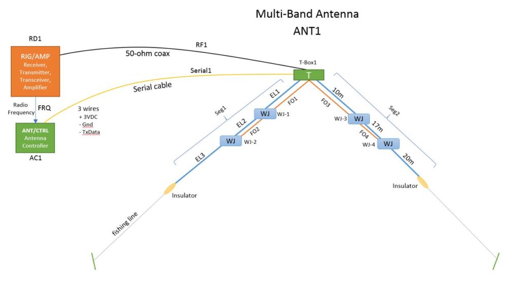
The Serial1 control cable consists of 3 wires: 1) 3 VDC power, 2) a ground return, and 3) a TxData serial data signal in RS-232 or RS-485 compatible format, running at a 19.2K baud data rate. The Serial1 signal reaches T-Box1 “T”, whereby it is converted from an electrical serial data signal into a corresponding lightwave signal using a Fiber Optic Transmitter (which is a fiber LED transducer). The light signal is then conveyed via plastic fiber optic cables FO1 and FO3 into respective WJ junction boxes (aka. “Wireless J-Box”) WJ-1 and WJ-3 simultaneously.
Why plastic fiber optics? Plastic fiber optics were chosen for several reasons:
- Inexpensive
- Capable of generating a small “wake-up” signal remotely (solves the low-current MCU wakeup problem when band-switching is needed)
- Readily available from typical parts houses
- Flexible enough to bend readily and not break from nominal stretching
- Durable enough to withstand extreme heat, sub-zero freezing, icing, wind and moisture.
This fiber optic signal is then repeated from WJ-1 as across fiber optic cable FO2 to WJ-3, where it terminates. Similarly, the fiber signal arriving at WJ-3 is duplicated and repeated to the next wireless J-box WJ-4. In this way, the control signals originating at AC1 arrive within milliseconds at each of the WJ box units to perform their function.
Figure 1 also shows a radio frequency signal RF1, which is bidirectional and flows via 50-ohm coaxial cable between the radio equipment RD1 and the antenna ANT1. ANT1 is a multi-band antenna comprised of multiple antenna element conductors organized into two segments, Seg1 and Seg2. Each antenna segment consists of multiple conductive elements EL1, EL2, and EL3. There can be any number of such conductive elements. As depicted in Seg 2, there are three such elements. The first is 10m, the 10-meter element. When the radio RD1 is tuned to a frequency within the 10-meter ham band, WJ-3 and WJ-1 along with WJ-4 and WJ-2 are all configured to the Open or disconnected state; i.e., the relays within each WJ box unit are opened. This results in only the 10-meter segments 10m on both Seg1 and Seg2 being connected via the RF1 coax to the radio RD1.
Whenever the radio operator switches the band or frequency of RD1 to a different band, for example, 20-meters, represented as 20m on Seg2, all four WJ boxes WJ-1, WJ-2, WJ-3, and WJ-4 will all switch their respective relays into the Closed or connected state; i.e., the relays within each WJ box unit are closed, thereby connecting all elements together within each segment. During 20-meter operation, Seg1 elements EL1, EL2, and EL2 are all connected electrically via the WJ box relays, creating a monoband antenna element along Seg1 that is resonant for 20-meter operation. Similarly, the 10m, 17m, and 20m elements shown on Seg2 are also connected to form a corresponding 20-meter resonant leg of the antenna system.
The net effect is to conjoin the proper set of elements together to create a monoband antenna that is tuned resonant for each of the target operating bands of interest. Given the relays are industrial grade specified to operate up to millions of times without failure, the overall antenna system should be more reliable than other multi-band antennas that require the use of stepper motors and other mechanical moving parts. And since the antenna is tuned to resonance effectively as a monoband antenna for each desired band of operation, no RF tuner is required to achieve acceptable SWR levels and excellent radiation efficiency. The use of relays instead of active trap components reduces losses and corresponding radiation gain reductions associated with traditional trap-based designs.
A two-segment dipole antenna is shown in Figure 1 as ANT1. Antenna elements can be used as elements within a dipole (as shown), inverted-vee, vertical, or as driven (or passive director/reflector) elements in a Yagi-Uda antenna or any other antenna design. Each antenna segment is labeled Seg1 and Seg2.
Please note that Figure 1 represents just one possible embodiment, where the ANT CTRL function AC1 is separated by an electrical serial cable Serial1 from T-Box1. In other cases, both the T function of T-Box1 and ANT CTRL functions can be combined into a single antenna controller, embodied within a Raspberry Pi, Arduino, or other intelligent device using wireless signals such as WiFi, Bluetooth, ISM-band, or other radio wave control signals to connect remote serial data signals from the antenna controller to the radio device, which can be located far away from each other.
Based upon the signals provided by the Antenna Controller, the J-Box switching devices will open or close their relays to reconfigure their respective conductor elements. Each J-Box may also repeat the control signal to another J-Box that is adjacent to the J-Box to ensure the original control signal reaches all J-Box devices along each antenna segment. It’s also possible to configure one or more J-Boxes to act purely as optical fiber signal repeaters for situations requiring much longer fiber optic runs; i.e. longer antenna elements on lower HF bands like 160 meters, for example.
The switched segment(s) could just as easily have been used to create other antenna configurations, including but not limited to verticals, inverted-vees, Yagi-Uda, or any other common antenna topology. The key aspect of this invention is that a traditional antenna’s conductive elements can be subdivided into multiple sub-elements, whereby the sub-elements can be reconfigured using the J-Box switching devices to shorten or lengthen the overall antenna. WJ boxes units can be used to control active or passive elements of an antenna.
For example, in a Yagi antenna, you have many elements positioned along a boom: driven elements that are directly connected to the coaxial cable (via WJ-box switching devices), along with passive elements called reflectors and directors, which can also be switched in and out to resonance to improve the overall gain of a multi-band Yagi antenna. This approach to Yagi design results in fewer conductive elements being required, potentially reducing weight and wind load.
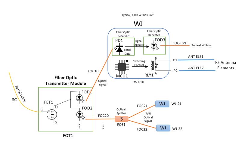
Figure 2A depicts two antenna controllers AC1 and AC2. AC1 combines T1, the fiber optic transmitter module, directly with the antenna controller module. AC2 depicts the separation of the antenna controller module from fiber optic transmitter T2. AC2 and T2 are connected together via serial cable SC, which operates as discussed earlier and is shown in Figure 1.
The orange lines FOC1 and FOC2 represent fiber optic cables that carry the light signals from the transmitter module T1 to WJ-1. WJ-1 contains a repeater module that first receives the incoming light signal from FOC1, converts it into an electrical signal inside of WJ-1, then converts it back into a second outbound light signal carried by FOC2 to WJ-2. In the original embodiment, there can be up to 16 of these WJ box units, each connected in series with the next along an antenna segment. AC1 can receive its frequency signal from wired, wireless, or direct signaling using a computer such as a PC, Mac, Raspberry Pi or other computer.
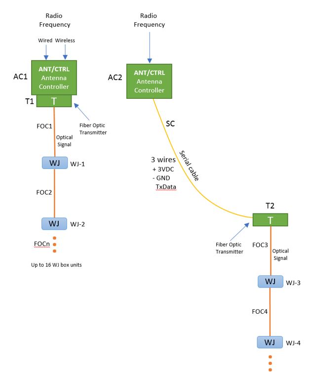
AC2 shows an antenna controller connected to a fiber optic transmitter T2 via the serial cable SC, a 3-wire cable of #24 insulated wire. An RS-232 signal configured to operate at a standard baud rate, such as 19.2 Kb, is used to convey signals from the antenna controller AC2 to the optical transmitter T2. T2 then converts the electrical serial data signal into corresponding light signals using photo LEDs, which are connected to FOC3 to carry the optical signal to WJ-3. WJ-3 repeats that signal via FOC4 to WJ-4 and so on down the line for as many WJ box units as needed.
Block diagram Figure 2B shows the operation of a Fiber Optic Transmitter Module labeled FOT1. FOT1 receives an incoming signal, such as the serial data signal SC, which flows through FET1, which is used as a current switch to drive one or more photo LEDs. Figure 2B shows two photodiodes FOD1 and FOD2, which are simultaneously driven with the serial data signal, thereby converting the electrical signal into a light signal. The light signal from LED FOD1 flows into optical cable FOC10 and into WJ-10. The signal converted by FOD2 flows into FOC20 which is connected to an optical splitter box S labeled FOS1. FOS splits the light signal in half, so it is thereby routed through both FOC21 and FOC22 to reach WJ-21 and WJ-22 respectively. The splitting of optical signals is convenient for reducing the number of fiber optic cable runs required to drive more complex antenna configurations, such as Yagi antennas with many segments and elements.

WJ-10 is typical of how each WJ box unit operates. Inside each WJ box is a fiber optic receiver module that uses a photodiode, shown here as PD1, or a phototransistor (not shown). The photodiode PD1 converts the light energy received from the plastic fiber optic cable FOC10 into a corresponding electrical signal. That electrical signal is then amplified and filtered, generating two resultant signals shown in Figure 2B as Signal Repeater flowing from PD1 into FOD3 and Serial Data flowing from PD1 into MCU1.
The Signal Repeater signal drives the Fiber Optic Repeater FOD3, which creates a new light signal that flows out of WJ-10 as FOC-RPT. This repeated signal is a near duplicate of the original light signal FOC10, which is cascaded down the line to the next WJ box along the antenna segment.
The first such Serial Data signal flowing from PD1 to MCU1 causes the microcontroller to wake up from a low-power deep sleep state. The next serial data packet that arrives contains the switching command along with the desired frequency. The MCU makes a switching decision, then commands relay RLY1 to either open or close.
RLY1 is a 1-coil latching relay, so once it has been switched into a given state, it remains there with no further power or attention being required. The relay contacts A and B of RLY1 connect to P1 and P2, respectively. P1 and P2 are the RF ports connecting the antenna elements ELE1 and ELE2 to the relay contacts. When RLY1 contacts are in the closed position, ELE1 and ELE2 are connected, thereby lengthening the overall antenna segment. When RLY1 contacts A and B are open, ELE1 and ELE2 are isolated, shortening the antenna segment and disconnecting the two elements.
Upon completion of a switching operation, which takes up to 20 milliseconds, MCU1 reverts into its low-power deep sleep state. This saves an enormous amount of power consumption because the light signal can be used to remotely awaken MCU1 anytime there is something to do. Most of the time MCU1 is sleeping, consuming 1 microamp or less power. This low power operation makes multi-band, switched antenna operation possible using two (2) standard AA or AAA batteries, which can operate for 10 to 20 years or longer with no maintenance or intervention. The actual duration of service depends upon temperature conditions and battery characteristics. Energizer Ultimate Lithium batteries were chosen due to their 20-year shelf-life guarantee and wide operating temperature range.
The wake-up and control signals sent over fiber optics provide the ability to convey low-power wake-up signals to these remote devices, which solves a major drawback with the use of RF wake-up methods, which suffer from distance limitations and/or consume far too much power to convey the wake-up signals. The remote wake-up signaling aspect over non-conductive medium is one of the key innovations which make this antenna viable for real-world use.
In other embodiments and prototypes, rechargeable batteries were also used. The energy was harvested from both solar power via solar cells and via RF energy harvesting from the actual RF energy of the antenna itself. These energy harvesting circuits proved expensive and space-consuming, so they have been omitted from the latest embodiment, almost doubling the cost per WJ box unit. The latest version of the invention has achieved extremely low power operation due to the use of light over fiber optics for wake-up and communications instead of the RF wireless operation present in the earlier designs. However, there may be cases where rechargeable batteries and/or supercapacitors could prove useful and so are not excluded from potential future designs.
Schematic, Electronic Design, and Operation
Figure 3 is a schematic of the Optical J-Box switching device. Schematic, PCB Layout and Parts Lists are available using EasyEDA. The Antenna Switch section is comprised of an RF Switch, a 1-Coil Latching Relay, Panasonic model #ASW1103HLW, labeled RL1. RL1 is used to switch the radio frequency (RF) signal across mounting pads P1 and P2. These mounting pads connect the J-box PC board traces to conductive stainless-steel bolts, which connect the antenna signals flowing across the two antenna element conductors for switching purposes. This relay consumes up to 67 ma for 5 to 10 milliseconds during each switching operation.
RL1 is controlled using H-Bridge Relay Driver U2. U2 applies the proper relay control currents in the correct polarity to open or close relay RL1. Relay control decisions are provided to U2 by U1, the Antenna Control MCU (microcontroller unit), a Microchip PIC16LF18345 device. This PIC processor was chosen due to the sizable amount of data and program space needed, along with its low power operation and USART functionality. There are many functions and spare pins that are not used.
The MCU acts as the local switching controller for the Optical J-box unit. Digital signals flow from pins 2 (RA5) and 1 (RA4) to the H-Bridge U2 device, whereby relay open and close signals are applied as needed.
The MCU U1 also provides visual activity signaling via LED1 via pin 10 (RB7). LED1 provides signaling by flashing visual dots and dashes in Morse code to indicate the status of the MCU and its operation, which is useful for diagnostic and troubleshooting.
MCU U1 uses digital input signals from SW1 to configure which frequency band this J-Box unit will be responsible for managing. The user sets the four DIP switches to a setting to indicate where along with the antenna system or elements this J-Box participates. This DIP switch configuration can represent either a frequency band (e.g., 20-meter ham band) or a unique identifier for this J-Box for direct addressing. A value of zero (all DIP switches turned off) indicates this J-Box unit will not perform any switching and is purely a signal repeater. The four DIP switch settings are interpreted by the MCU firmware as a single number from 0 to 15.
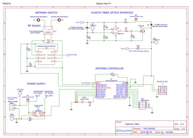
The Plastic Fiber Optics Interface circuitry provides optical-electrical signal conversions. Photodiode D1 receives a fiber optic signal from a plastic fiber optical cable, containing wake-up and control signals from the main Antenna Controller transmitter. The light signal striking D1 generates a small electrical current, in the range of 20 to 150 millivolts, across resistor R4. The magnitude of the electrical signal depends upon the power of the original fiber optic signal, reduced by plastic fiber optic cables losses across many meters of fiber optic cable, connectors, and other ambient losses.
Note that the energy captured by photodiode D1, an Industrial Fiberoptics D91B photodiode, originated outside of the J-Box itself at the main Antenna Controller device. It is this remote energy transfer via fiber optics that enables the low-power wake-up signal to be conveyed over significantly longer distances than is traditionally available via radio frequency wake-up methods. Note this optical signal is itself considered a very low-power signal, in the range of a few hundred microwatts flowing across plastic fiber optic cable.
The millivolt-level signal from D1 at TP1 enters the plus pin 3 of U4, a signal comparator. Actual measurements of the received signal’s voltage across R4 were observed to be 750 mV over a 1-meter length of GH4001 plastic fiber optic cable. Observed signal voltage dropped about 3 dB, as expected, over a 10-meter cable distance, due to the expected loss of 0.3 dB per meter of plastic fiber optic cable.
The longest typical run of plastic fiber cable on a typical quarter wavelength multiband 160-80-40-20-15 meter dipole is the 80-40 meter segment, which is about 10 meters or 33 feet.
The comparator’s reference voltage on the minus pin 4 is approximately 7 millivolts, as created by the voltage divider R11 and R12. When the comparator senses the increased voltage signal on its “+” terminal, its output on pin 1 rises to a high state (about 2.5 volts with a 3V VCC3 voltage on pin 5). In turn, this high signal is applied to the gate of Q1, the BSS128 enhanced-mode n-channel MOSFET transistor, causing it to conduct.
When Q1 conducts, it creates current flow through D2, a photo LED which produces an outgoing fiber optic light signal that is a near duplicate of the original signal, repeated for use by the next J-Box unit that can be connected in series along the antenna segment. JP2 can be used to disable this repeater function, thereby reducing the overall current drain on the battery. Q1 inverts the signal received on its gate pin, creating an inverse signal at its drain output. This signal is used to wake up MCU U1 via its’ ExtIn GPIO port on pin 18. ExtIn is programmed to wake up MCU U1 from its low-power sleep state. This same signal is also present on pin 17, the RxData pin, which is connected to the USART inside of MCU U1.
Upon waking up, MCU U1 reads the wake-up signal, a few characters of text that gets discarded. This allows the MCU’s clock oscillator to come up to full speed, in preparation for receiving the asynchronous serial data control signal that will arrive a few milliseconds later. That control signal contains information that is used to make a switching decision based upon the Band Select SW1 setting. The incoming serial data packet contains protocol markers, an opcode value, two operand values, and a 16-bit CRC that’s used for error checking.
The MCU verifies the message is authentic and unmodified by computing its own 16-bit CRC from the received data packet and comparing it with the CRC value received within the packet. If it is a valid packet, then the MCU proceeds with processing the packet as a command. The most common command is OPCODE_SWITCH_FREQ, which tells the MCU to use Operand 1 as a frequency value, then look up the corresponding band. If a valid band is found, then the received frequency is compared with the band setting from the lookup operation, and a switching decision is made.
If the frequency received via the data packet is greater than or equal to the lookup frequency (the band this J-box is intended to control), then the relay is commanded to open; otherwise, the relay will be closed. This switching operation, along with similar switching actions performed by the other peer J-Box units along each antenna segment, will reconfigure the antenna system to operate correctly at the frequency contained in the data packet.
Optionally, the LED1 may flash to indicate which switching operation is taking place (in diagnostic mode only). Without LED use, measured MCU consumption is about 2.5 ma for 20 ms. During that 20 ms period, the relay switching operation is estimated to consume up to 67 ma, but actual switching occurs so quickly that it is not observed on the digital ammeter.
Finally, to ensure the lowest possible current drain during long periods of inactivity, the J-Box Power Supply utilizes U3 as a power switch. U3 is used to switch 3V power, provided by two Energizer Ultimate Lithium AAA batteries at operating temperature ranges of -40C to +140C, which is estimated to provide power for up to 20 years during regular and heavy contesting operation. Alternatively, it is estimated that a switching device can also operate on a CR2032 coin cell for up to 7 years at -30C to +140C.
By removing Jumper J1, current measurements were taken regularly to identify any potential power consumption issues. During sleep, the entire system has been shown to consume just 1 to 1.5 uA. This ultra-low power consumption during normal antenna operation and periods of inactivity is the key to multi-year battery life.
Switched power is turned on and off as needed to power H-Bridge U2 and the relay RL1. The control signal from MCU pin RC5 is used to enable/disable voltage flow through U3 to create VCC3SW. This power is turned on each time the MCU wakes up to a received signal to process it and turned back off before the MCU goes back to sleep.
The MCU is configured to run its watchdog timer during low power sleep mode, awakening once every 33 seconds and then immediately going back to sleep. This ensures the MCU will always be operational and never require manual intervention, should RF, lightning, static charges, or other stray interference somehow affect the MCU’s normal operation. For example, if the MCU were running during a nearby lightning discharge that caused a power spike that disrupted the MCU, the watchdog timer will fire within 33 seconds and reboot the MCU.
Prototype Package
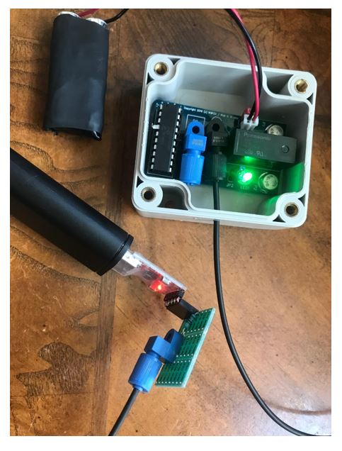
Below is a picture of an early prototype, caught while LED is signaling a switching operation. At the bottom is the transmitter module, connected to the USB cable and USB to TTL adapter.
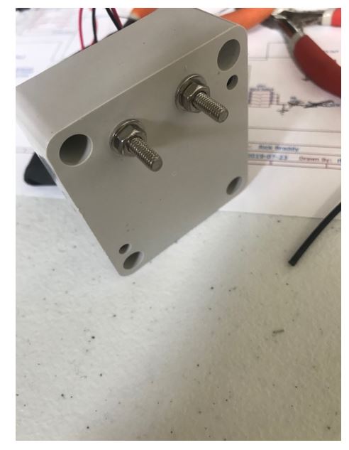
Below is picture of the stainless-steel antenna RF connection terminals outside the enclosure. In final production units, the PCB and all components, except the config switch, should be sealed using a thin, transparent layer of weatherproof sealant. All bolts and other holes will be sealed with silicon and the entire unit will be painted with a UV-resistant sealant to reflect sunlight to reduce heating and prolong the device’s well-being.
Improvements on Pre-Existing Inventions
Most multi-band antennas compromise peak efficiency by making tradeoffs to achieve their multi-band operation. Trapped antennas require active inductor and capacitor components which reduce the antenna’s radiated power, thereby reducing gain on transmit and sensitivity on receive. Other multi-band antennas such as G5RV and OCF (off-center fed) dipoles require the use of a tuner to compensate for non-resonance to match impedance with the transmission line.
Other multi-band antennas, such as the SteppIR, vary the length of the conductive elements to achieve resonant operation by using mechanical stepper motors that drive a spool of conductive tape or wire that is lengthened or shortened to achieve resonance. These mechanical parts are prone to periodic failures and require maintenance, and are costly antennas to acquire, build and maintain.
This invention overcomes these limitations by using fixed-length antenna sub-elements, which when combined, form truly resonant antenna configurations that have similar characteristics to monoband antennas. There are no moving parts or mechanical components to fail, except the relays. The relays used as switching devices are rated for hundreds of thousands to millions of operations, far more than the expected number of operations over the entire lifetime of the antenna system.
The extremely low power requirements, on the order of a few microamperes when idle and up to 75 milliamperes for 20 milliseconds or less during infrequent switching operations, enable each J-Box to operate for up to 10 to 20 years on today’s common lithium batteries.
The use of nonconductive fiber optics to generate the wake-up signal and convey the control signals used to reconfigure the antenna system is the key to enabling the long battery lifespan and communicating with the antenna switching devices located directly on the antenna structure, without interfering with normal antenna operation. The use of fiber optics avoids interference with the normal operation of the antenna elements due to its ability to convey wake-up and control signals over non-conductive media.
Other Uses or Applications for This Invention
The method described for sending wake-up and control signals over fiber optics can be used to connect remote devices that must operate for lengthy periods of time on battery operation at very low power levels. The ability to convey wake-up signals to these remote devices solves a major drawback with the use of RF wake-up methods, which suffer from distance limitations and the use of too much power to convey the wake-up signals when an edge or remote devices must operate on battery at very low power levels for years at a time.
Specific areas for further review
The following areas have been identified as needing peer review to determine whether additional safety margin or other protective measures may be required.
- RFI Shielding – will the common mode currents invoked by several thousand watts of RF energy near the endpoints and along the antenna segments conducted through the latching relay interfere in any way with the normal, low power operation of the device? Early testing of a prototype device has not shown any indication of RF interference at 100-watt level.
- Comparator Hysteresis – is 7 mV enough protection against RFI or other potential surges that could trigger the comparator, which then awakens the MCU and powers D2 up with an outbound spurious optical signal, thereby awakening every other device down the line?
- Relay RFI Suppression – in earlier prototypes, adding C1 across the relay control lines eliminated much of the RFI with the system. Is this enough protection? Is use of a varactor to further suppress static discharges from nearby lightning needed to protect the circuitry?
- The AAA battery leads – contains 6-inch wire leads to flow from the battery onto the PCB connector terminals. Should these battery inputs be protected against common mode currents with a low pass filter or other protection?
- PCB Shielding – is a Faraday cage required to protect the circuitry from the strong electromagnetic near field, given the MCU is always asleep during RF transmit operation, and common mode currents should be relatively constant across all PCB traces; i.e.., minimal differential voltage drops due to common mode current? To keep costs down and simplify configuration of the device, no shielding is currently used.
Conclusions
Multiband, truly resonant antenna operation has been sought after for decades. Few multiband antenna designs have delivered fully resonant operation without some types of tradeoffs, usually tradeoffs in antenna gain or performance on some of the supported bands.
The Switched Multi-Band Antenna addresses many of the historical limitations of traditional antenna designs. As with most things in life, there is no free lunch. To get the benefits of true resonance for multi-band operation, the tradeoffs entail added complexity and components vs. a simple wire or trap antenna design.
Time will tell whether or not these tradeoffs are truly worthwhile. It has been a very worthwhile journey of discovery and learning for me, learning MCU firmware development, some interesting electronic design adventures, and fun prototyping it all and testing the various antenna designs to arrive at this one.
I truly hope this information turns out to be useful and somehow helps us advance the state of amateur radio. Should there be interest, I am happy to release the firmware source code under the same license for general use.
Rick / W5FCX

Do you do contact form blasting to get sales? If you do I can provide you with lists of millions of verified contact forms. If you don’t I can show you how I did it on your website contact form just now and it’s easy for you to do it too. For details add me on Skype and let’s chat, my ID is: live:.cid.7aad4787a72a11d0